
ADVANCING THE PICK & PLACE FRONTIER
A domestic supplier of core equipment for advanced packaging of AI chips — panel-level packaging, memory, HBM and 2.5D/3D process flows.
- 40KUPH
- World-leading panel DA throughput
- ±5μm
- Placement accuracy
- 20+
- Years of packaging equipment experience
- 20+
- Patents in advanced packaging
FOUR CORE BUSINESS AREAS
Conventional Semiconductor Packaging
High-speed epoxy silver-paste die bonders, fully automatic chip sorters, and complete conventional packaging line solutions.
Advanced Semiconductor Packaging
For panel-level and 2.5D/3D processes: die-stacking thermo-compression bonders, FOPLP ultra-high-speed DA, and TC Bonders that raise yield and throughput.
High-End Equipment Customisation
End-to-end service from architecture design to finished machine, built to your line layout and technical specification — modules or complete systems.
Machine Retrofit & Maintenance
Retrofit and maintenance for Japanese (Canon, Hitachi, Toshiba, Fasford) and Taiwanese (GPM, GMM) platforms — extending service life and lowering operating cost.
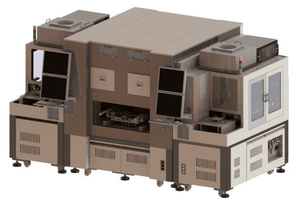
Bonder
All Models
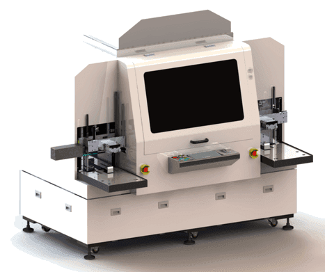
D-MARS PLUS
D-MARS PLUS
2nd-generation DAF die bonder for DRAM memory
- 3500UPH
- Throughput
- ±10μm
- Accuracy @3σ
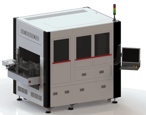
D-MARS 6600
D-MARS 6600
DAF thermo-compression die bonder
- 2500UPH
- Throughput
- ±15μm
- Accuracy @3σ
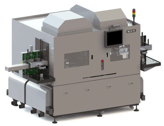
D-MARS FC
D-MARS FC
General-purpose flip-chip die bonder
- 6000UPH
- Throughput
- ±5μm
- Accuracy @3σ
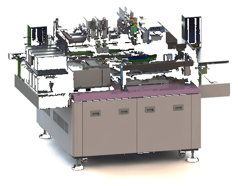
D-MARS HS
D-MARS HS
High-speed epoxy (silver paste) die bonder
- 15000UPH
- Throughput
- 250ms
- Cycle Time
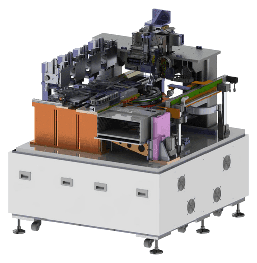
Rushes A12
Rushes A12
Fully automatic chip sorter
- 500ms
- Cycle Time
- 3Bin
- Output Zones
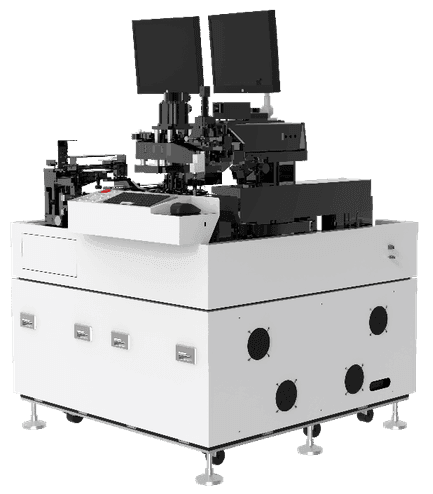
Rushes S12
Rushes S12
Semi-automatic chip sorter
- 6KUPH
- Throughput
- 600ms
- Cycle Time
FROM ITRI TO DOMESTIC SUBSTITUTION
- 2000
Team formed
Founding team formed at Taiwan's ITRI; began the first localisation research on semiconductor packaging equipment in Taiwan, with technology transfer study at Hitachi in Japan the same year.
- 2004
Taiwan's first DAF machine
Developed Taiwan's first DAF platform, benchmarked against the Hitachi DB 700 series. Shipped to SPIL and ASE in the same year.
- 2006
Taiwan's first glass bonder
Developed the GS 700 glass bonder for camera modules.
- 2009
AOI capability established
As mobile camera shipments scaled, developed a CHIP GAP inspection machine and built the AOI technology team.
- 2011
Hsinchu plant completed
New Hsinchu facility established, providing volume production capability.
- 2014
CIS Bonder in production
CIS Bonder shipped in volume to camera module makers including Sunny and Q Technology.
- 2019–2024
Rooted in mainland China
Expanded the semiconductor packaging and camera module product lines into mainland China.
- 2022
DaheSemi founded
DaheSemi (Shenzhen) Co., Ltd. established in March 2022.
CORE TECHNOLOGY
High-Speed, High-Precision Pick & Place
Precision lead-screw linear drive modules, linear motor drives, voice-coil force control, and low-stress pickup of small, ultra-thin die.
High-Precision Motion Stages
XY and XYZT multi-axis platforms with ±2.5μm absolute planar accuracy.
Vision, Alignment, Metrology & Inspection
Fully replaces manual visual inspection with quantified, data-driven results — detecting particle coverage, die chipping, cracks, foreign matter and colour non-uniformity.
Die Stacking
High-precision multi-layer die stacking technology.
Algorithms, Simulation & Modal Analysis
Motion control algorithms with structural simulation and modal analysis.
2.5D / 3D Process Technology
Silicon interposer fabrication, TSV, TCB and CoWoS process technology.
CUSTOMERS & PARTNERS









LET'S TALK ABOUT YOUR PROCESS.
Tell us about your line, your die and your yield targets. Our engineering team will come back with a concrete equipment proposal.